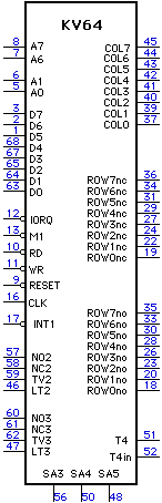
KV64 - Velocity Sensitive Keyboard Scanner

Pin Description

Bus Interface

Pin #

Name

I/O

Description

8
A7
Input
active high
Address Bus bit 7 or CE1+
7
A6
Input
active low
Address Bus bit 6 or CE2-
6
A1
Input
Address Bus bit 1. Register selection
5
A0
Input
Address Bus bit 0. Register selection
3
D7
Bidirectional
Data Bus 7
2
D6
Bidirectional
Data Bus 6
1
D5
Bidirectional
Data Bus 5
68
D4
Bidirectional
Data Bus 4
67
D3
Bidirectional
Data Bus 3
65
D2
Bidirectional
Data Bus 2
64
D1
Bidirectional
Data Bus 1
63
D0
Bidirectional
Data Bus 0
12
IORQ or CE3-
Input
active low
Z80 IORQ or Chip Enable
13
M1
Input
active low
Z80 M1 or connect to Logic High
10
RD
Input
active low
Read Enable
11
WR
Input
active low
Write Enable
9
RESET
Input
active low
Master Reset
16
CLK
Input
System Clock. 20MHz max.
17
INT1
Output
Open collector
Interrupt. Connect to Z180 Int1 pin


Key Matrix Interface

Pin #

Name

I/O

Description

45
COL7
Output
active high
Column Drive 7
44
COL6
Output
active high
Column Drive 6
43
COL5
Output
active high
Column Drive 5
42
COL4
Output
active high
Column Drive 4
41
COL3
Output
active high
Column Drive 3
40
COL2
Output
active high
Column Drive 2
39
COL1
Output
active high
Column Drive 1
37
COL0
Output
active high
Column Drive 0
36
ROW7nc
Input
active high
ROW 7 Normally Closed
34
ROW6nc
Input
active high
ROW 6 Normally Closed
31
ROW5nc
Input
active high
ROW 5 Normally Closed
29
ROW4nc
Input
active high
ROW 4 Normally Closed
27
ROW3nc
Input
active high
ROW 3 Normally Closed
24
ROW2nc
Input
active high
ROW 2 Normally Closed
22
ROW1nc
Input
active high
ROW 1 Normally Closed
19
ROW0nc
Input
active high
ROW 0 Normally Closed
35
ROW7no
Input
active high
ROW 7 Normally Open
33
ROW6no
Input
active high
ROW 6 Normally Open
30
ROW5no
Input
active high
ROW 5 Normally Open
28
ROW4no
Input
active high
ROW 4 Normally Open
26
ROW3no
Input
active high
ROW 3 Normally Open
23
ROW2no
Input
active high
ROW 2 Normally Open
20
ROW1no
Input
active high
ROW 1 Normally Open
18
ROW0no
Input
active high
ROW 0 Normally Open


Expansion

Pin #

Name

I/O

Description

56
SA3
Output
Address Drive for external multiplexer
50
SA4
Output
Address Drive for external multiplexer
48
SA5
Output
Address Drive for external multiplexer
57
NO2
Input
Expansion Input for external multiplexer
58
NC2
Input
Expansion Input for external multiplexer
59
TV2
Output
Data Drive to external shift register
46
LT2
Input
Data Input from external shift register
60
NO3
Input
Expansion Input for external multiplexer
61
NC3
Input
Expansion Input for external multiplexer
62
TV3
Output
Data Drive to external shift register
47
LT3
Input
Data Input from external shift register


Utility

Pin #

Name

I/O

Description

51
T4
Output
Timing Clock Drive for internal and external shift registers
52
T4in
Input
Clock for internal shift registers. Must be connected to T4
53
TEST
Output
Do not connect
54
MODE
Input
Connect to Gnd
4, 21, 25, 38, 55
Vcc
Power
+5V supply
14, 15, 32, 49, 68
Gnd
Power
0V supply


Notes
  • 1) There are Ground and Power pins on each side of the package. It is recommended that at least two sides are closely decoupled with multilayer ceramic 0.1µF capacitors.

  • 2) All Row inputs should have pull down resistors to Ground. The value determines the settling time of the diode/switch matrix, for scanning rates of 1ms a maximum value of 22k is suitable and this should be reduced for faster scan rates.

Internal Registers

The KBV64 registers are I/O mapped and decoded as a block from 80h to DFh, addresses 80h to 83h are used and multiply mapped within the block. If finer mapping is required the A6 and A7 pins may be used as chip enables gated by external decoding logic.

  • Write Register 0 Int1_Control mapped at 80h
    • Bit 0 = Interrupt Enable
    • Bits 1-7: Not Used

    Interrupts are generated at any key address if the contact is moving or was on the previous scan. This algorithm gives all the key states that need to be responded to. The interrupt routine should read the Scan Status Registers of the matrices being scanned and then the Scan Address Register.

  • Write Register 1 Scan Rate Prescaler mapped at 81h

    Sets the 8 bit division ratio N or the Bus Clock B MHz.
    Scan Time, T = ( N+1 ) * 1024/B

    For a scanning repeat rate of 1ms:
    N = ( 0.001/1024 * B ) - 1
    or roughly:
    B (in MHz) - 1
    so if the System clock is 10MHz load the Prescaler with 9.

  • Write Register 2 Mode Register mapped at 82h
    • Bit 0: Mode0
    • Bit 1: Mode1
    • Bits 2-7: Not Used

    Mode0 and Mode1 are fully decoded to give four scanning modes affecting matrix 2:

    Mode1
    Mode0
    Mode Description
    0
    0
    Full Scanning
    0
    1
    73 Note Scanning
    1
    0
    76 Note Scanning
    1
    1
    88 Note Scanning

    In the 73, 76 and 88 Note Modes the scanning of Matrix 2 is inhibited when out of range to reduce the number of external components necessary.

  • Read Register 0 Scan Requests mapped at 80h

    Contains a bit map of the matrix sections causing an interrupt.

    • Bit 0: keys 0 - 63
    • Bit 1: keys 64 - 127
    • Bit 2: keys 128 - 191
    • Bits 3 to 7: always 0

  • Read Register 1 Scan Address mapped at 81h
    • Bits 0-5: Row/Column Address of the key(s) causing an interrupt. The scanning is halted until this register is read.
    • Bits 6, 7: always 0

  • Read Register 2 Scan Status 1 mapped at 82h
    • Bit 0: NC1 (internal)
    • Bit 1: NO1 (internal)
    • Bit 2: LT1 (internal)
    • Bit 3: 0
    • Bit 4: 1
    • Bit 5: 0
    • Bit 6: 1
    • Bit 7: 0

    The upper 4 bits form a test pattern "5xh" for checking the chip is present.

  • Read Register 3 Scan Status 2 mapped at 83h
    • Bit 0: NC2 (external pin)
    • Bit 1: NO2 (external pin)
    • Bit 2: LT2 (external pin)
    • Bit 3: 0
    • Bit 4: NC3 (external pin)
    • Bit 5: NO3 (external pin)
    • Bit 6: LT3 (external pin)
    • Bit 7: 0

    The Scan Status three bit patterns give the following conditions:

  • LT
    NO
    NC
    Key Status Description
    0
    0
    0
    Preset - contact has just left the NC position
    0
    0
    1
    Rest - no interrupt
    0
    1
    0
    Hold - contact is at rest in NO position - no interrupt
    1
    0
    0
    Trav - contact is travelling between NC and NO positions
    1
    0
    1
    Off - contact has just reached NC position
    1
    1
    0
    Trigger - contact has just reached NO position


Specifications and information presented in these pages may change in the interests of continuing product improvement. No responsibility can be accepted for misinterpretation of the information provided.

EUREKA, KV64 and Z80-DIO are trademarks of Hinton Instruments.
Z80 and Z180 are trademarks of Zilog Inc.
All other manufacturers trademarks are acknowledged.


Copyright ©2002 Hinton Instruments
Last updated: 25 January 2007