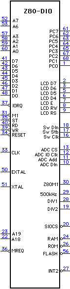
|
Bus Interface
|
|||
|
Pin #
|
Name
|
I/O
|
Description
|
|---|---|---|---|
|
52
|
A7
|
Input
active low |
Address Bus bit 7 or CE1-
|
|
53
|
A6
|
Input
active high |
Address Bus bit 6 or CE2+
|
|
57
|
A3
|
Input
|
Address Bus bit 3. Register selection
|
|
58
|
A2
|
Input
|
Address Bus bit 2. Register selection
|
|
59
|
A1
|
Input
|
Address Bus bit 1. Register selection
|
|
60
|
A0
|
Input
|
Address Bus bit 0. Register selection
|
|
41
|
D7
|
Bidirectional
|
Data Bus 7
|
|
42
|
D6
|
Bidirectional
|
Data Bus 6
|
|
43
|
D5
|
Bidirectional
|
Data Bus 5
|
|
44
|
D4
|
Bidirectional
|
Data Bus 4
|
|
45
|
D3
|
Bidirectional
|
Data Bus 3
|
|
46
|
D2
|
Bidirectional
|
Data Bus 2
|
|
47
|
D1
|
Bidirectional
|
Data Bus 1
|
|
48
|
D0
|
Bidirectional
|
Data Bus 0
|
|
37
|
IORQ or CE3-
|
Input
active low |
Z80 IORQ or Chip Enable
|
|
31
|
M1
|
Input
active low |
Z80 M1 or connect to Logic High
|
|
35
|
ST
|
Input
|
Z180 bus signal
|
|
40
|
RD
|
Input
active low |
Read Enable
|
|
39
|
WR
|
Input
active low |
Write Enable
|
|
34
|
RESET
|
Input
active low |
Master Reset
|
|
33
|
CLK
|
Input
|
System Clock. 20MHz max.
|
|
23
|
A19
|
Input
|
Address Bus bit 19. Memory Map Decoder
|
|
22
|
A18
|
Input
|
Address Bus bit 18. Memory Map Decoder
|
|
36
|
MREQ
|
Input
active low |
MREQ. Memory Map Decoder
|
|
17
|
INT2
|
Output
Open collector |
Interrupt. Connect to Z180 Int2 pin
|
|
Port Interfaces |
|||
|
Pin #
|
Name
|
I/O
|
Description
|
|
61
|
PC7
|
Bidirectional
|
Port C Bit 7
|
|
62
|
PC6
|
Bidirectional
|
Port C Bit 6
|
|
63
|
PC5
|
Bidirectional
|
Port C Bit 5
|
|
64
|
PC4
|
Bidirectional
|
Port C Bit 4
|
|
65
|
PC3
|
Bidirectional
|
Port C Bit 3 / Shaft Encoder 2 Input B
|
|
67
|
PC2
|
Bidirectional
|
Port C Bit 2 / Shaft Encoder 2 Input A
|
|
68
|
PC1
|
Bidirectional
|
Port C Bit 1 / Shaft Encoder 1 Input B
|
|
1
|
PC0
|
Bidirectional
|
Port C Bit 0 / Shaft Encoder 1 Input A
|
|
2
|
LCD D7
|
Bidirectional
|
LCD 4 bit Data Bus bit 7/3
|
|
3
|
LCD D6
|
Bidirectional
|
LCD 4 bit Data Bus bit 6/2
|
|
5
|
LCD D5
|
Bidirectional
|
LCD 4 bit Data Bus bit 5/1
|
|
6
|
LCD D4
|
Bidirectional
|
LCD 4 bit Data Bus bit 4/0
|
|
7
|
LCD E
|
Output
|
LCD Enable
|
|
8
|
LCD RW
|
Output
|
LCD Read/Write
|
|
9
|
LCD RS
|
Output
|
LCD Register Select
|
|
18
|
Sw Din
|
Input
|
Switch Data Input
|
|
17
|
Sw Stb
|
Output
active high |
Switch Strobe (Parallel Load)
|
|
16
|
Sw Clk
|
Output
|
Switch Clock
|
|
13
|
ADC CS
|
Output
|
ADC Chip Select
|
|
12
|
ADC IO Clk
|
Output
|
ADC I/O Clock
|
|
11
|
ADC Add
|
Output
|
ADC Address
|
|
10
|
ADC Din
|
Input
|
ADC Data Input
|
Glue |
|||
|
Pin #
|
Name
|
I/O
|
Description
|
|
30
|
Z80M1
|
Output
|
Z80 M1 for Z80 bus
|
|
29
|
500kHz
|
Output
|
CLK ÷20 (for MIDI UARTs)
|
|
28
|
DIV2
|
Output
|
CLK ÷10 (for ADC System Clock)
|
|
19
|
DIV2
|
Output
|
Programmable Divider Output (Square Wave)
|
|
20
|
CS
|
Output
active low |
Chip Select for second I/O mapped peripheral
|
|
24
|
RAM
|
Output
active low |
RAM Chip Select for Memory Mapped SRAM
|
|
26
|
ROM
|
Output
active low |
ROM Chip Select for Memory Mapped EPROM
|
|
56
|
FLASH
|
Output
active low |
FLASH Chip Select for Memory Mapped FLASH Device
|
|
50
|
EXTAL
|
Input
|
Oscillator or External Clock input
|
|
51
|
XTAL
|
Output
|
Oscillator Drive for external Crystal (20MHz max)
|
|
Utility |
|||
|
Pin #
|
Name
|
I/O
|
Description
|
|
54
|
MODE
|
Input
|
Connect to Gnd
|
|
4, 21, 25, 38, 55
|
Vcc
|
Power
|
+5V supply
|
|
14, 15, 32, 49, 68
|
Gnd
|
Power
|
0V supply
|
Notes
1) There are Ground and Power pins on each side of the package. It is recommended that at least two sides are closely decoupled with multilayer ceramic 0.1µF capacitors.
Internal Registers
The Z80-DIO registers are I/O mapped and decoded as a block from 40h to 5Fh, addresses 40h to 87h are used and multiply mapped within the block. If finer mapping is required the A6 and A7 pins may be used as chip enables gated by external decoding logic. A second peripheral may be I/O mapped from 60h to 7Fh using the CS pin.
- Write Register 0 Port A - ADC Control mapped at 40h
- Bit 0 = ADC Address
- Bit 1 = ADC I/O Clock
- Bit 2 = ADC Chip Select
- Bits 3-7: Not Used
- Write Register 1 Port B - Switch Shift Register Control mapped at 41h
- Bit 0 = Switch Clock
- Bit 1 = Switch Strobe
- Bits 2-7: Not Used
- Write Register 2 Port C Data Out mapped at 42h
- Bit 0 = PC0
- Bit 1 = PC1
- Bit 2 = PC2
- Bit 3 = PC3
- Bit 4 = PC4
- Bit 5 = PC5
- Bit 6 = PC6
- Bit 7 = PC7
- Write Register 3 Port D LCD mapped at 43h
- Bit 0: not used
- Bit 1: LCD RS
- Bit 2: LCD RW
- Bit 3: LCD E
- Bit 4 = LCD4
- Bit 5 = LCD5
- Bit 6 = LCD6
- Bit 7 = LCD7
- Write Register 4 Port C Control mapped at 44h
Bits 0-7 control the direction of PC0-7, similar to a Z80-PIO port in Bit Mode. 0 = output 1 = input.
- Write Register 5 Port D LCD Control mapped at 45h
- Bits 0-3: not used
- Bits 4-7 control the direction of LCD4-7, 0 = output 1 = input
- Write Register 6 Divider Constant mapped at 46h
Bits 0-7 set the time constant of the programmable divider. 00h = ÷256
- Write Register 7 Int2_Control mapped at 47h
- Bit 0 = Interrupt Enable
- Bit 1 = Shaft Encoder 1 Interrupt Enable
- Bit 2 = Shaft Encoder 2 Interrupt Enable
- Bit 3 = Clock Select: 0 = EXTAL, 1 = CLK
- Bits 4-7: Not Used
- Read Register 0 Port A - ADC Data mapped at 40h
- Bit 0 = ADC Din
- Bit 1-7: not used
- Read Register 1 Port B - Switch Data mapped at 41h
- Bit 0 = Sw Din
- Bit 1-7: not used
- Read Register 2 Port C Data Input mapped at 42h
- Bit 0: PC0 / Shaft Encoder 1A
- Bit 1: PC1 / Shaft Encoder 1B
- Bit 2: PC2 / Shaft Encoder 2A
- Bit 3: PC3 / Shaft Encoder 2B
- Bit 4: PC4
- Bit 5: PC5
- Bit 6: PC6
- Bit 7: PC7
- Read Register 3 Port D - LCD Data Input mapped at 43h
- Bit 0-3: not used
- Bit 4 = LCD4
- Bit 5 = LCD5
- Bit 6 = LCD6
- Bit 7 = LCD7
- Read Register 7 mapped at 47h
Bits 0-7: not used. Reading this port clears the interrupt request status.
Specifications and information presented in these pages may change in the interests of continuing product inprovement. No responsibility can be accepted for misinterpretation of the information provided.
EUREKA, KV64 and Z80-DIO are trademarks of Hinton Instruments.
Z80 and Z180 are trademarks of Zilog Inc.
All other manufacturers trademarks are acknowledged.